PCA9540BD driver for arduino + breakout boards schematics
Introduction
For an other side project in electronics, I wanted my arduino to communicate with two ADXL345 accelerometers. The protocol used to communicate with these device is I2C, and a problem I encountered was that both my accelerometers had the same I2C address. This is a problem because the I2C address of each device in a closed circuit must be unique in order to prevent any disturbance.
After looking on the internet, I found that the PCA9540BD component was what I needed. PCA9540BD is a 2-channel I2C-bus multiplexer, meaning it can redirect the SCA and SDA pins to (SCA0, SDA0) or (SCA1, SDA1) depending on the instruction it receives. One advantage of the component is that it is controlled using the I2C protocol too, limiting the number of pins it uses. It has 8 pins in total : VDD, VSS, SCA, SDA, SCA0, SDA0, SCA1, SDA1.
Implementation of the driver for arduino
The first problem was that there wasn't any existing PCA9540BD driver for the arduino, so you had to directly use the Wire library in order to communicate with the component (though it didn't take a lot of lines). Thus, my first modest contribution has been to write a driver for this component. It is open source and availalble on github.
Design of two breakout boards
The second problem was that the PCA9540BD pins have a pitch of 0.05 inches making the component difficult to connect to a prototype board. As far as I know, there doesn't exist any breakout board for this component. I first used a DIP8 adapter, but this solution was far from perfect, since the pins' order and the lack of any labelling made my circuit less understandable.
That is why I decided to design my own breakout boards (using Eagle) and printed them on 10 PCBs using Seeedstudio. I tested two designs, and both of them worked perfectly.
Breakout board : big version
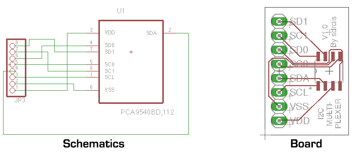
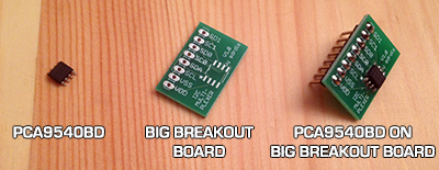
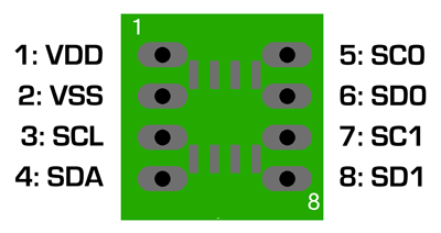
First, I designed a bigger version, where I conveniently labelled each pin in order to improve the readabibility of my circuit. The schematics are open source and available in this repository.
Breakout board : compact version
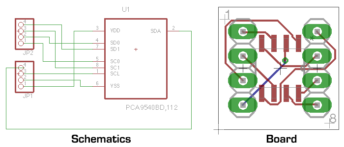
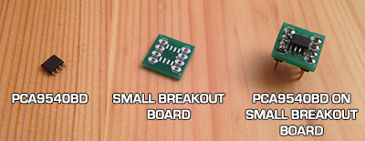
I also designed a more compact version. Though I didn't have any room to write labels, I changed the order of the pins in order to make the board more convenient compared to a classical DIP8 adapter : in this board, all pins that must be connected to the arduino are on one side, and all pins that must be connected to the devices are on the other side. The schematics are open source and available in this repository.
Conclusion
This first published project in electronics allowed me to familiarize myself with the arduino library architecture as well as with PCB design. On a side note, I must improve my soldering skills for this kind of boards, as I used a classical soldering iron, and it was very difficult, especially for the compact breakout board, not to solder two pins near to each other. I plan to use solder paste and solder stencils in the future for this kind of problem (see this video for instance).